This project was made modular composed by 3 boards, analog board, interface board and main control (Android tablet). This was made like this because I had some boards with a pic micro that also could control the analog board as in first design and to reduce the cost of the analog board.
The boards are connected according the diagram, as show the tablet communicates with the interface board via I2C bus that also is used by the tablet for reading the RTC. The interface board controls the analog board by two PWM signals one for current and the other for voltage, a digital out select between PS and DL.
All analog voltages are read by the ADC in the interface board and sent to tablet when requested.
Here we can see all boards connected making charging an discharging tests on a Li-ion battery.
On the software side things got complicated I started to using ADK based on Eclipse and creating a simple interface to communicate with the I2C bus.
Since java doesn't allow communications with i2c bus, I had to write the interface using JNI (java native interface) in C to make the bridge between the Android app and the hardware, all of this is only possible on a rooted device.
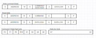
With the interface working all that the application had to do is send commands for reading an writing using the protocol bellow.
This protocol uses 3 bytes for writing (example setting pwm value) as mentioned 10bits are written to the registers specified on the remaining 6bits of data high byte.
Before reading data the corresponding register must be set, so a prior write with the register address is needed, after that any read sequence will return data from the that register.
For the interface board I used a pic16f76, this pic as many others has a dedicated MSSP port that can be configure to operate as I2C slave device.
At start the device configures i2c port and start the control state machine. this machine handles all data received.
If an address was received, next the R/W bit on the slave address is tested if set (Read Data) then data H byte is sent and state is now RDL.
On the Acknowledge of data H from master, the device sends data L and enters on IDLE state.
As for characterization curves of the output voltage, they are not that great as the graph shows, but keeping in mind that all parts are low end and no care on stability was taken this project works as expected
All project files are on git and design here


Sem comentários:
Enviar um comentário